The consumer demand for compact, miniaturized, and smart electronic devices is making electronics manufacturers use the smallest available packaging footprints. As a result, Printed Circuit Board Assemblies (PCBAs) have become denser and more sophisticated than ever. The real challenge then becomes how to achieve consistency and reproducibility in the printing process of these sophisticated PCBs.
To ensure consistency and reproducibility, the electronic manufacturers make use of stencils to deposit solder paste to PCBs. Inevitably, the condition of the stencil now becomes the Key Performance Indicator (KPI) governing the efficiency, consistency, and reproducibility of the PCB printing process. Almost 70% of defects in Surface Mount Technology (SMT) are attributed to imperfections in depositing solder paste. Therefore, it becomes imperative to study, improve, and monitor the stencil cleaning process.
This article throws light on the criticality of cleaning stencils before solder paste deposition followed by some methods to decontaminate stencils. To educate the readers, some standard stencil cleaning practices are mentioned. Finally, some products from Techspray are highlighted which aid process engineers in thorough stencil cleaning.
Why Clean Stencils?
A stencil is a metal sheet with tiny apertures used for depositing solder paste on PCB substrate in very small areas i.e., SMT pads. The squeegee presses the solder paste into the stencil apertures for proper deposition as shown in Figure 1.
In the electronics industry, the cleanliness of PCB substrates has traditionally been a focus area, resulting in substantial profits for those manufacturers of PCB cleaning products. What is often overlooked is the stencil cleaning process. What if the stencils are not properly cleaned before the stencil printing process? Dirty stencils would result in an undesirable volume of solder paste deposited to the SMT pad and this is categorized as a printing fault. A misprinted PCB could be disqualified during inspection requiring extra cost for repair and rework.
In electronics manufacturing, around 40% of production time is wasted on debugging printing issues [1]. Some major issues caused by contaminated stencils include slumping, open solder joints, shifting, smearing, and solder bridging. To avoid such issues, it is mandatory to control the volume of solder paste transported to PCB pads, particularly for fine, ultra-fine, chip-scale, BGA, and flip-chip components.
Technically, it is characterized by transfer efficiency (TE), which is defined as the ratio of the actual solder paste volume deposit to the volume of the corresponding aperture [1].
Ideally, TE should be 100% but a TE of 70% is also acceptable. To maintain the desired value of TE, the stencil apertures must be properly cleaned and free of any leftover solder paste/residue. Figure 2 portrays an example of a stencil with clogged apertures. Figure 3 shows the negative impact of printing with clogged stencil apertures.
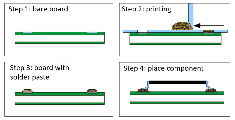
Figure 1: Stencil printing process [2]
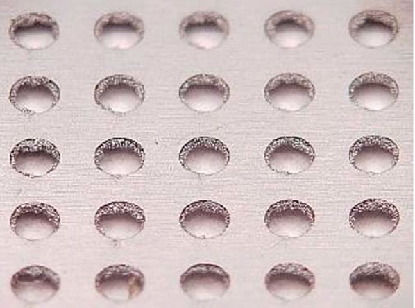
Figure 2: A contaminated stencil [3]
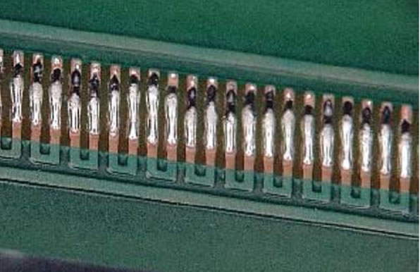
Figure 3: Open solder joints due to insufficient solder paste [3]
Similarly, a stencil with residue on its bottom side will lead to inconsistent transfer of paste to the PCB pads. Leftover solder paste on the underside of the stencil gets transferred to the other board and causes bridging. Therefore, cleaning the stencil removes residue, decreases printing problems, and ensures the uniformity of the prints. Proper stencil cleaning makes the electronics manufacturing business more profitable as the need for rework is minimized. A little extra effort at the beginning of a process saves time and money in the long run.
How To Maintain Stencil Cleanliness?
Under Stencil Wiping:
The stencil-printing machine often does the job of under-stencil wiping (dry, wet, or vacuum wipe). A cleaning solvent is used with a lint-free paper to remove the solder paste. To achieve the best cleaning results in under stencil wiping, the flux component must be dissolved within the solder paste. This eases the release of solder spheres which are then easily collected by wiping paper [4].
These printers also include a vacuum generator that sucks the contamination from the apertures. If the printer does not have such an automated system, under stencil wiping can be performed manually using a pre-saturated lint-free wipe. However, manual stencil cleaning has its own drawbacks, which include risks to workers’ health, the risk of damage to the stencil itself, and the reliance on the operator’s experience. These drawbacks often outweigh what benefits there may be to manual cleaning.
Ultrasonic Agitation:
Ultrasonic agitation is performed by generating ultrasonic waves (40 kHz) in a liquid cleaning medium [3]. This process (called cavitation) forms bubbles in the liquid that reach even the tiny apertures of the stencil. The bubbling action provides the mechanical force to separate contaminants from the stencil. Higher frequencies can result in better cleaning but the exposure time to moisture increases which could harm the stencil adhesive bonds. It is therefore a standard practice to use the “sweep” feature or multiple frequencies [3].
A key point is that the cleaning tank must be of stainless steel. Plastic tanks have the tendency to absorb ultrasonic waves and may render the cleaning process inefficient. Finally, the cleaning chemistry must be chosen properly. The cleaning agent must be compatible with the stencil material. The main advantage of ultrasonic cleaning is that there is no chance of damage to the stencil as 40 kHz vibrations are completely safe for the stencils. Moreover, this process takes less time to complete as compared to the manual cleaning process.
Spray-In-Air Technology:
As the name suggests, this technology uses a spray pump and nozzles to spray the washing solution onto the stencil. The flux is placed in the solution resulting in solder balls lifting off the stencil [5]. The spray pressure must be high enough to remove all solder balls from the apertures and yet low enough to not damage the delicate stencils.
Batch Stencil Cleaning:
A short description of this process is already available in this article by Techspray. In the case of aqueous cleaning, a rise in temperature improves the effectiveness of the cleaning process and reduces cleaning time. However, too high a temperature (generally over 110oF) can delaminate stencil adhesive [3]. Too low a temperature increases exposure time to moisture which may reduce the strength of the adhesive bond and frame interface.
Nano-Coatings:
Besides ensuring reduced bridging problems and improved solder paste release, nano-coatings are well known to reduce the need for underside cleaning of stencils. These coatings (1-100 nm thick) prevent spreading of solder paste on the underside of stencils. Basically, the nano-coatings are meant to provide the advantage of “fluxophobicity” i.e., it allows the solder paste to de-wet and be removed from the stencil easily [6]. The fluxophobicity can be estimated by measuring the contact angle. In [6], it has been experimentally proved that nano-coatings improve the contact angle as compared to uncoated stencils. The increase in contact angle is due to the de-wetting of the solder paste from the stencil underside. A visual comparison of a coated and uncoated stencil is shown in Figure 4 and Figure 5. However, before making the final decision, the process engineer must also consider the fact that nano-coatings can alter the properties of stencil material [2]. Another useful point to keep in mind is that nano-coatings perform well when the apertures are very small and the solder paste is dense.
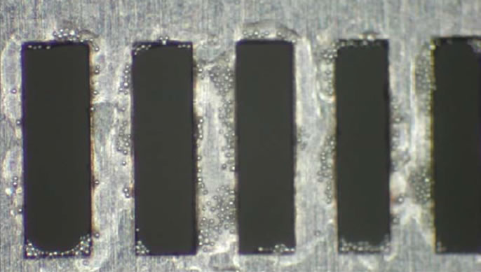
Figure 4: Bottom of uncoated stencil after 20 prints [6]
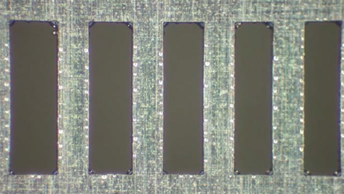
Figure 5: Bottom of coated stencil after 20 prints [6]
Techspray’s Line of SMT Cleaning Products
Techspray since 1968 has made the electronics manufacturing process more profitable, efficient, reliable, safer, and environmentally friendlier. Techspray’s products are now used worldwide in all electronic applications involving aviation, heavy industry, plant, and equipment maintenance. Being an industry leader, Techspray offers an extended line of SMT cleaning products for cleaning PCBAs, misprinted boards, stencils, squeegees, and equipment surfaces.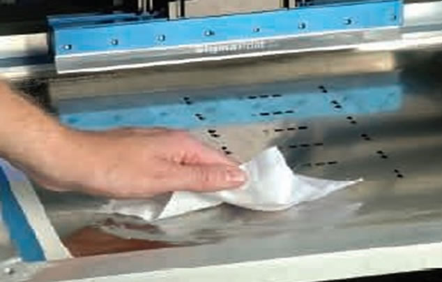
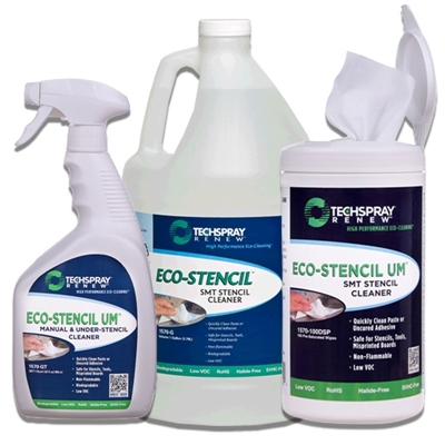
ECO-STENCIL UM CLEANER is an ultimate replacement for IPA cleaners used to clean stencils, squeegees, and misprinted boards. It is non-flammable, removes all type of solder pastes and is best suited for batch ultrasonic cleaning.
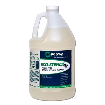
ECO-STENCIL RF CLEANER is a rinse-free, non-flammable cleaner to wipe the underside of contaminated stencils. Its unique amalgam of solvent and DI water is effective in removing all type of solder pastes and adhesives. This product also finds its application in spray-in-air stencil cleaning.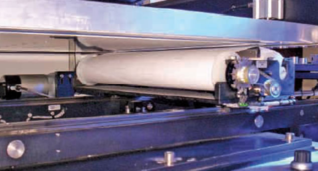
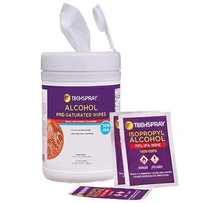
TECH ROLL UNDERSTENCIL WIPE with minimum lint level is a good choice for wiping the underside of stencils. It is capable of both wet and dry wiping of stencils.
All these products are RoHS compliant and environmentally friendly with no Volatile Organic Compounds (VOC) and do not contribute to global warming. Moreover, these cleaners provide good cleaning performance at ambient temperatures and above.
For more information, contact your Techspray application specialist at 678-819-1408 or [email protected].
References
[1] S. W. Y. Nourma Khader, "Stencil Printing Process Optimization to Control Solder Paste Volume Transfer Efficiency," IEEE Transactions on Components, Packaging and Manufacturing Technology, vol. 8, no. 9, pp. 1686-1694, 2018.
[2] M. D. Robert Kay, "A review of stencil printing for microelectronic packaging," Soldering & Surface Mount Technology, vol. 24, no. 1, pp. 38-50, 2012. [3] IPC, "IPC - Build Electronics Better," 2007. [Online]. Available: https://shop.ipc.org/ipc-7526/ipc-7526-standard-only/Revision-0/english. [Accessed 17 12 2022].
[4] Kyzen, "ON PRINTER UNDERSTENCIL WIPE CLEANING," Kyzen, [Online]. Available: https://kyzen.com/industries-applications/electronics-assembly-cleaning/stencil-cleaning-misprinted-pcb-cleaners/understencil-wiping-cleaning/. [Accessed 17 12 2022].
[5] M. Konrad, "Stencil Cleaning: Choices and Proven Strategies," Semiconductor Digest, [Online]. Available: https://sst.semiconductor-digest.com/2003/08/stencil-cleaning-choices-and-proven-strategies/. [Accessed 17 12 2022].
[6] T. Lentz, "Can Nano-Coatings Really Improve Stencil Performance?," FCT Assembly, Greeley.