Faulty or damaged electronics assemblies obtained after batch processing is a big setback for not only the electronics manufacturers who are competing in the market, but also for the process engineers. With the increasing use of Surface Mount Technology (SMT) most defects in new electronics assemblies are credited to unoptimized solder reflow profiles.
To educate PCB design engineers, this article aims to elaborate how to achieve optimal solder reflow profiles and avoid common Printed Circuit Board Assembly (PCBA) defects, e.g., bridging, tombstoning, beading, and cracking during manufacturing. Some state-of-the-art products of Techspray will be highlighted to aid engineers to achieve optimal reflow profiles and fault-free PCBAs.
Owing to an increase in market competition, modern electronics manufacturers are focusing on optimizing the cost, size, and manufacturing process of electronics assemblies. SMT has been able to provide them with all these luxuries. Geometrically, SMT devices are smaller in size, which makes PCB miniaturization achievable and they reduce spurious inductances and capacitances which makes PCBA less vulnerable to Electromagnetic Interference (EMI) thus increasing overall system reliability. Moreover, since SMT components can be soldered to both sides of PCB, achieving high board density becomes easier as compared to through-hole components. Therefore, SMT devices have emerged as the popular choice among modern electronics manufacturers. Most importantly, SMT devices do not require conventional soldering procedures, instead they use reflow soldering process which allows for the ease of automation.
Solder Reflow Process
First step in solder reflow process is the application of solder paste on metal pads. Solder paste is an amalgam of flux and solder. Flux ensures cleaning of pads i.e., removing oxides and impurities, and wetting of molten solder. Due to the sticky nature of flux, it also acts as an adhesive and holds SMT devices in place before a permanent bond is formed. Solder melts (reflows) to form a permanent bond between the component lead and the PCBA pad. This is achieved in a reflow oven with three temperature regions:
- Pre-heating
- Soaking
- Reflowing
Afterwards, the PCBA is allowed to cool.
Electronics manufacturers procure a dedicated solder reflow oven, which has multiple temperature regions to control the soldering process and the board moves to each region by means of a conveyer belt. The required thermal profile for optimal solder reflow profile is pre-programmed to achieve full automation.
A pre-requisite to solder reflowing is the proper printing of solder paste onto PCBA pads. Solder paste is applied on pads with the help of stencils. PCBA stencil, shown in Figure 1, is a thin sheet of material (brass or stainless steel) with holes and apertures oriented according to the pattern of PCB under consideration. A properly designed stencil ensures the deposition of solder paste to achieve solder joints with excellent electrical connection and mechanical integrity.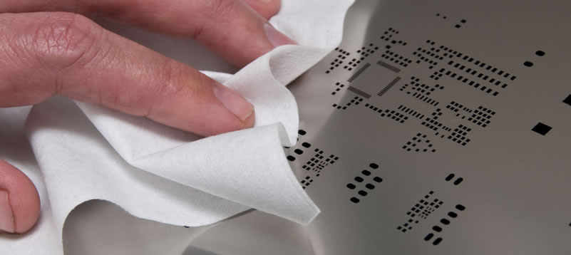
Figure 1: A clean Stencil for depositing solder paste
Cleaning in Solder Reflow Process
Almost 70% of solder defects arise due to faulty printing of solder pastes [1]. Therefore, in SMT devices, stencil cleaning determines the key success of resultant PCBAs. Fine pitch lands like BGAs and other advanced packages place new challenges on stencil cleaning. Failure to do proper cleaning during or after the reflow process causes partial or complete plugging of stencil apertures as shown in Figure 2 and deposition of non-reflowed solder paste/residues on the bottom side of stencil as shown in Figure 3.
The solder residue may get deposited on subsequent PCBAs resulting in incorrect or poor solder placement. This inappropriate deposition of solder paste becomes the reason for most common PCBA defects like bridging, solder beading, tombstoning, and open solder joints. Therefore, to ensure efficient and quality production, engineershave to continuously monitor and inspect the condition of stencils.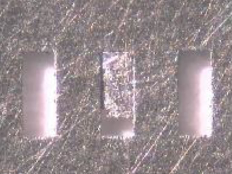
Figure 2: Partially plugged stencil apertures [3]
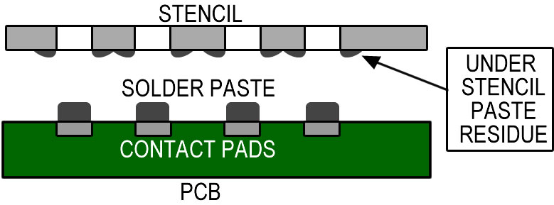
Figure 3: Dirty stencil bottom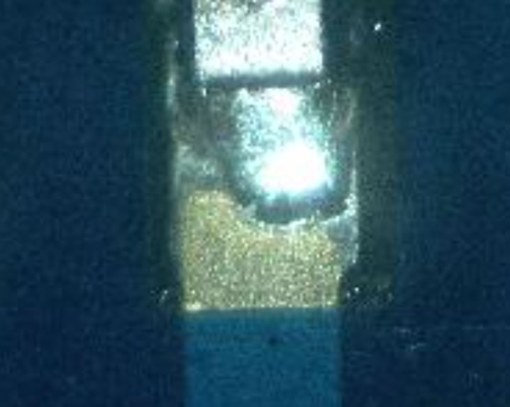
Figure 4: Insufficient solder joint due to partially blocked apertures [3]
For the above-mentioned reasons, stencil cleaning has become a necessary practice during printing in PCBAs. Stencil cleaning requires removal of all solder particles/residues without damaging the stencil itself. There are three primary methods of stencil cleaning:
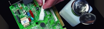
Under Stencil Wiping
The under-stencil wiping process demands cleaning each stencil’s bottom using a cleaning solvent and lint-free paper. Most modern printers provide an automated system to perform under stencil-wiping making this the most common. A vacuum system extracts unreleased solder paste from apertures reducing the chances of open solder joints in the final PCBA as shown in Figure 4. This reduces maintenance by filtering particulate within the lint-paper while a porous solvent bar wets the paper through osmosis reducing residual cleaning solvent.
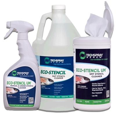
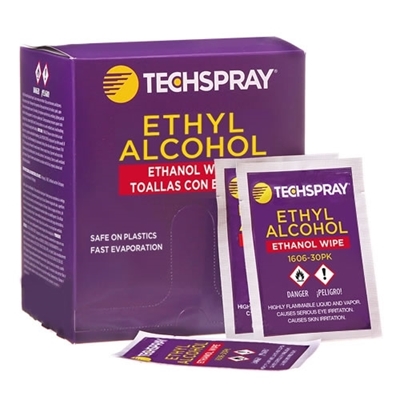
With 40 years of successful experience in electronic cleaning, Techspray offers a full line of High Performance Eco-Cleaning products. Techspray’s Eco-stencil UM (1570)is an ideal replacement for Isopropyl Alcohol (IPA) cleaners, which may be prohibited due to safety and environmental restrictions for VOC emissions or waste disposal issues. Eco-Stencil UM is nonflammable and effectively removes all types of solder pastes from misprinted PCBAs and stencils.
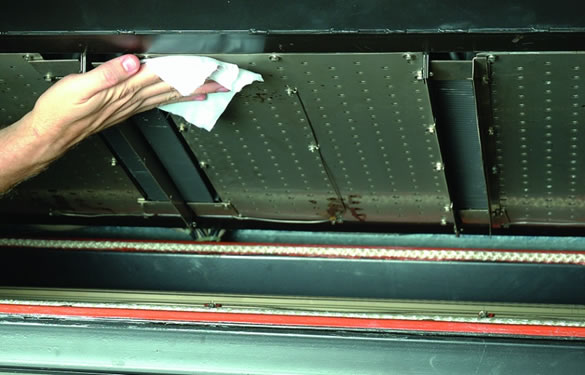
Manual Stencil Cleaning
In the absence of an automated cleaning system, manufacturers may use a manual wipe process to clean stencil bottoms. However, because there is no vacuum sucking the apertures could remain contaminated. Compressed air may blow out particulates but could damage the delicate apertures or even the stencil. Moreover, solder particles may spread onto personnel, equipment or surfaces, or even nearby PCBAs blocking vias or causing short circuits.
Due to an increased risk of exposure to heavy metals, and flammable chemicals, manual cleaning is not recommended as it poses serious threats to health and safety of operators. Techspray’s Eco-stencil UM(1570)is an ideal replacement for IPA cleaners, which may be prohibited due to safety and environmental restrictions for VOC emissions or waste disposal issues. Importantly, its nonflammable nature makes it risk-free for operators to use it during manual stencil cleaning.
Batch Stencil Cleaning
According to IPC, batch cleaning equipment represents the largest installed electronics assembly cleaning processes. They encompass several specific cleaning technologies and through-put capabilities.Batch machines are very similar to dishwashers. As the name suggests, batch machines clean batches of stencils and misprinted PCBAs in a single cycle to increase process efficiency.
At the end of a reflow shift, stencils are put in the automated batch cleaning machine. These use a suitable chemical solvent, then initiate a rinse cycle, then finally dry the stencils via convection radiant heat and rapid air exchange.
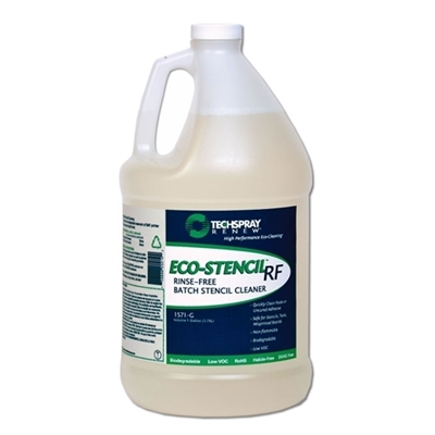
With 40 years of successful experience in electronic cleaning, Techspray offers a full line of stencil cleaners. Eco-stencil RF Batch Stencil Cleaner (1571-G) is an effective non-flammable drop-in replacement for isopropyl alcohol (IPA) or other solvents commonly used in rinse-free batch stencil cleaning systems. Its unique water-based blend is effective at removing a wide variety of pastes and adhesives. Higher concentrations can be used for more difficult pastes and adhesives. It can also be used as a manual or under-stencil cleaner discussed earlier.
Reflow Oven Cleaning
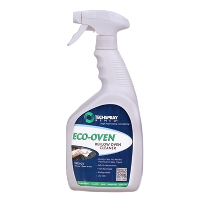
While most defects in PCPAs are attributable to improper solder application, a crucial stage is in the reflow process itself. After the reflow process is completed, solder fluxes and gas emissions are deposited inside the SMT reflow oven. Increasing level of remnant precipitates and gas emissions can disturb the temperature distribution inside the oven, which results in unstable reflow profiles. Therefore, regular cleaning of reflow ovens maintain desired reflow profiles. Techspray’s Eco-Oven Cleaner (1573-QT) is non-flammable and offers very effective cleaning against all types of flux residues.
How To Achieve Best Reflow Profile?
To achieve best quality solder joints, the reflow soldering process itself has to be optimized. An unoptimized reflow profile can give rise to defects like bridging, tombstoning, voiding, poor wetting, solder beading, and even component cracking [2]. A standard reflow profile is shown in Figure 5. Optimized reflow profiles generally have less ramp rate in the preheating and reflow zones as compared to standard profiles. Selecting the best reflow profile for an application demands making a trade-off between overall heat input to PCBA and the ramp rates without compromising the quality and safety of the final product.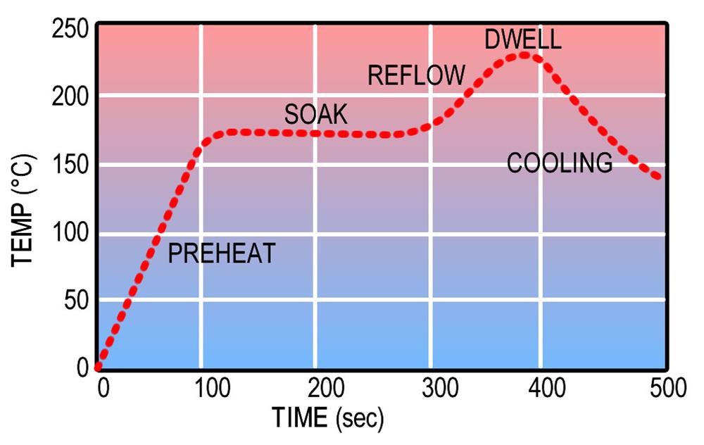
Figure 5: A standard reflow profile
In standard reflow profiles, ramp rate is higher during preheating, therefore a common defect induced in PCBAs is called solder bridging (i.e., the solder paste slumps due to decrease in viscosity caused by thermal agitation)[2]. In such cases, it is preferable to use semi-optimized reflow profiles. In standard reflow profiles as shown in Figure 5, a sudden increase in temperature profile after the flat soak region may cause defects like tombstoning and solder beading.
One way to avoid these defects is to increase the temperature in soak region. However, this will increase overall heat input to the PCBA and may damage electronic components. An improved approach may be to make the temperature profile in soak region a slow ramp up instead of a flat line. This will prevent excess heat input as well as any sudden ramp up. Final adjustment in profile of soak region is subjected to the temperature difference between component leads and the PCB.
Generally, less wetting time and reduced peak temperatures result in good quality solder joints. However, in some applications higher peak temperatures may be required. In this case, to prevent some components from extreme heat, Techspray offers WonderMASK, which is the leading temporary solder mask in the electronics industry. It can withstand temperatures up to 343oC.
Finally, the cooling rate must match the heating rate set in the reflow region for proper solder joint formation.
Techspray at Your Service for PCBA Rework
Bridging, the most common defect, can cause the components to fail if it is not resolved prior to board testing. Bridging might cause a short circuit between two leads of a component. This is shown in Figure 6. Removing this excess solder is necessary and one of the easiest desoldering techniques is the use of soldering wick or soldering braid. Soldering wick is a coil of copper strands. Being an excellent conductor of heat, heating copper braid will absorb the excess solder through capillary action.
Techspray wick has been a mainstay at PCB rework, repair and prototyping stations for over 30 years. Techspray offers rosin pre-fluxed copper braid (RoHS compliant) to repair such PCBAs and are equally effective on lead and lead-free solders. Pro-wick Desoldering Braids of Techspray meets MIL-F-14256 criteria and provides the quickest wicking action in PCBA repair environments.
Moreover, Techspray also offers desoldering iron tips. High-quality Plato desoldering iron replacement tips increase desolder speeds and decreases the total cost. Higher temperatures and high tin content solders, common in lead-free solder processes, place additional strain on soldering iron tips. The long life of a Plato solder iron tip reduces tip changes, decreasing the total number of tips used and decreasing production time. The fast heat recovery of Techspray’s Desoldering Tipsfor SMT devices increase user effectiveness and has been a popular choice among electronics manufacturers for over 50 years.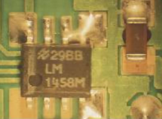
Figure 6: Solder Bridging example [3]
For more information on Techspray and Plato products, contact an application specialist at [email protected] or 678-819-1408.
References:
|
[1] |
IPC, IPC-7526 "Stencil and Misprinted Board Cleaning Handbook", Feb. 2007. |
|
[2] |
D. Bao, "Metallic Sources," [Online]. Available: https://metallicresources.com/wp-content/uploads/2017/02/n1.pdf. [Accessed 10 11 2021]. |
|
[3] |
NPL Defects Database. Available: http://defectsdatabase.npl.co.uk/defectsdb/defects_query.php |
|
|
|
|
|
|